The Importance of the Silk Screen in PCB Labelling
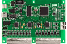
Silk Screen or Silkscreening is a significant step in the PCB (Printed Circuit Board) manufacturing process in which we print the legends viz the component reference (or value), test points, and signal names directly onto the PCB surface. This method mainly employs an ink that is capable of withstanding the harsh processes to which PCBs are subjected during assembly, such as soldering and cleaning. It prints typically component identifiers, test points, logos, warning symbols.
Improving Assembly Accuracy
One of the biggest advantages of PCB silk screen is to assist in the accuracy of the assembly process. Silk screening identifies component locations and orientations and human assembly errors are reduced in manual assembly of electronic components. An example is the polarity markings for diodes or capacitors, to help the technician place components in one way only (so that the risk of this assembly that can cause a circuit failure is minimized).
Boosting Aesthetics and Aiding Branding
Aside from the functionality, silk screening also adds to the aesthetic beauty of a PCB there is. Even when those screenprinting legends were crafted, those venerable PCBs would look, well, like something from years ago. Today's screenprinted PCBs are created using processes that are, to be polite, less optimized for the visual aesthetic. That's all changing though. New printer tech allows for multiple colors and finer text to be printed, ideal for consumer electronics where brand identity is everything. This feature allows for the addition of complex logos and branding elements which will help make the product quickly recognisable in a visual sense.
Resistance to Wear and Tear and the Elements
Silk screening inks are designed to withstand exposure to lots of things! These inks are formulated to resist fade, smear and chemical break down; which is important since PCBs are used across a range of environments. The markings are still legible even after exposure to high temperatures, moisture, and corrosive chemicals, ensuring the PCB can serve and diagnose correctly throughout its operational life.
Silk Boob Technological Advancements
Silk screening technology has come a long way resulting in more accurate, longer lasting marking than ever before. Silk-screening, as modern technology provides it, can create some incredibly detailed graphics at a resolution where the text is legible even under minimal magnification. High resolutions are key for the crowded PCBs utilized in smartphones and health-related devices, where space is at a premium and clearness is vital.
Complications of regulatory compliance and tracking
The printing of silkscreen shall be imperative for the compliance and traceability aspect as well. It enables traceability codes and regulatory markings (e.g., RoHS compliance symbols) to be included, as necessary for different markets. These signs tell all the regulations and standards required by the PCBs entirely, making the checkout process more gentle to entry the market as well.
In one of our more in-depth articles, we explore the necessity and purpose of silk screen in PCB design.
Silk screening on a PCB is about more than just adding some text and symbols; its a key piece in the design and build process that adds functionality, aesthetics, and compliance. PCBs on the whole are becoming more complex and miniaturized, and silk screen snuggles itself into a crucial niche of the industry, helping everyone in it meet high standards of quality and reliability.